Table Of Content
- ADALM2000 Activity: Audio Amplifier with Electret Microphone
- Why A²B Enables New and More Complex Data and Audio Transport Systems
- The Co-Fired Ceramic Fabrication Process
- Microcontrollers (MCUs) & processors
- Op-Amp Applications
- Why Do Digital and Analog Require Separate Ground Planes?
- To Design For High Speed Data Rates
The actual devices in any circuit are responding to continuously varying stimulus, so analog circuit design is really the foundation of the design of digital circuits. During the early days of analog circuit design, circuits were developed using hand-made schematics and calculations, without the possibility of simulating before testing. Nowadays, the hardware designer can rely on several digital tools to conduct a project. Schematic CAD (Computer Aided Design) tools can be used to design schematics from scratch.
ADALM2000 Activity: Audio Amplifier with Electret Microphone
This course provides a comprehensive introduction to various aspects of modern digital integrated circuit design. Navigate through the maze of tools, technologies and techniques including circuit components, component variations and practical design paradigms. Learn how to analyze, simulate and design a complementary metal oxide semiconductor (CMOS) analog integrated circuit. Analyze and simulate elementary transistor stages, current mirrors, supply- and temperature-independent bias and reference circuits. When the term “integrated circuit design” is mentioned, most people think of the design of complex microprocessors.
Why A²B Enables New and More Complex Data and Audio Transport Systems
The Daily Heller: Dafi Kühne's Analog Typographic Phantasma - PRINT Magazine
The Daily Heller: Dafi Kühne's Analog Typographic Phantasma.
Posted: Fri, 16 Feb 2024 08:00:00 GMT [source]
The professional resources include online lectures on how to do analog integrated circuit design step-by-step using design procedures. Since all the basic devices in an IC respond to continuous time stimulus, analog design forms the foundation for all IC design. There is significant variability in the manufacturing process for advanced technology nodes. The actual operation of the high number of devices on advanced ICs also causes variability.
The Co-Fired Ceramic Fabrication Process
This variability manifests as changes in operating voltage, operating temperature, and in performance. Densely packed devices can also interact with each other and with the silicon substrate, package, and board to cause signal distortions. All of these effects can occur between devices and within a single IC as well. Because analog design requires both intuition and rigor, each concept is first introduced from an intuitive perspective and subsequently treated by careful analysis.
Microcontrollers (MCUs) & processors
The central difference between analog and digital circuitry comes down to the way information is conveyed. An analog signal is continuous as opposed to the discrete high and low signals of a digital signal. Effectively, analog presents signals as they are, rather than a time-sampled representation. These signals represent a direct relationship between the parameters of the signal and whatever is being measured or generated - the signal is analogous to some physical phenomenon. Altering the characteristics of the signal, such as the voltage or frequency, induces a change in the output, or vice versa.
Simulation is an important step of electronic design, although it is sometimes neglected by engineers. Using simulations, one can tune the component values, adjusting them to achieve optimum performance. Also, different component models can be tested without needing to recalculate the model equations.
Efabless Announces the Inaugural Chipalooza Analog and Mixed-Signal Design Challenge - GlobeNewswire
Efabless Announces the Inaugural Chipalooza Analog and Mixed-Signal Design Challenge.
Posted: Thu, 15 Feb 2024 08:00:00 GMT [source]
The split ground plane helps ensure the signal integrity between analog and digital circuits doesn’t overly compromise one another through coupling. Because ground is ground, there must be at least one point where the analog ground (AGND) and digital (DGND) must be tied together. Often, this occurs directly at the component(s) in question by routing a short and direct trace between the pins. However, designers may want to avoid creating a single point that could lead to overly circuitous return paths. What is the best option for designers at this juncture, where seemingly contradictory best practices have to be reconciled?
Simulation programs can then be used to predict the circuit outcome before testing, calculating the signal behavior both in time and frequency. Some popular simulation tools in the market are the PSpice, LTSpice, Tina-TI and Multisim. Most designers quickly learn that routing over a split plane gap is a cardinal sin of signal integrity due to the large current loops formed by the return path, which can quickly lead to formidable EMI emissions. Back-to-back Schottky diodes can be utilized to help protect against a large enough potential developing between the AGND and DGND pins to prevent damage to the circuit. Ferrite beads can also be useful to create a passage at low frequencies while becoming highly resistive and functioning as an open at high frequencies. This low pass filter behavior ensures that low-frequency analog signals can easily flow between the separate ground planes while confining high-speed digital signals to their respective ground plane.
To Design For High Speed Data Rates
As mentioned, packages may contain internal analog and digital circuits, making the unified ground a nonstarter. This also glosses over other circuit constraints - even when bypassing the split ground is possible, juggling the placement and routing concerns of the full design may make it highly impractical. First, consider what components and circuits comprise a typical analog board.
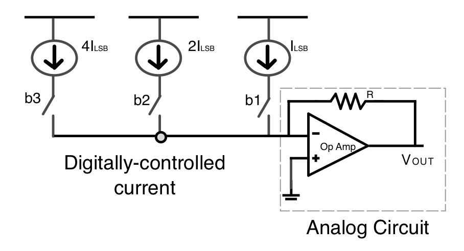
The behavior of the circuit is modeled in the time and frequency domains with attention focused on the fidelity/precision, consistency, and performance of the resultant waveforms. Circuit variability, both manufacturing and design induced, must be modeled and compensated for as well. Each data converter circuit below includes step-by-step instructions with formulas allowing you to adapt the circuit to meet your unique design requirements. We've provided at least one recommended data converter for each circuit, but you can easily swap it with another device if you've found one that fits better with your design. Our circuits require a basic understanding of data converter concepts, so if you are new to data converter design, we highly recommend reviewing our TI Precision Labs (TIPL) training series. ADC and DAC were briefly touched on above, but hopefully, the reader has noticed the inseparability of digital and analog design.
Simulation using a SPICE-like simulator is used to verify the clamp models. The second laboratory applies these ESD clamps to design, simulate, and verify the ESD input protection and output protection for an op amp. From the literature we know that second-order active filters can be implemented using the multiple-feedback topology, which requires only one OPAMP and several passive components (Figure 8). Now we need to define the OPAMP model and the value of the passive components. Further, methods exist for correcting this digital degradation that are simply unavailable to analog formats.


No comments:
Post a Comment